Ultra low noise regulators
In this section I would like to present some regulators, which can be successfully used for preamplifiers, DAC analog and digital parts.
1. Ultra low noise low-dropout regulator achieves 6-nV/√Hz noise floor
Every high-end fun meet already this apparently very simple, but in the reality complicated problem: to make very low noise power supply for his/her preamplifier. In practice you can find two big class of regulators - switching and linear. The advantages of switching supplies revolve around low weight, low material cost, and their ability to actively regulate at no additional cost. Bur that is just apparently! Noise is a potential problem with them, but is solvable by physically isolating and filtering the supply, in other words, by spending money, and as result the weight will be similar like linear regulators - just the efficiency is better. Usually degrade badly beyond their ratings the output with their noise. It helps if the power supply capacitors before and after the switcher are very substantial and with low ESR value. If you must be use them, their noise can be decreased if they are followed by a linear low noise regulator (with low dropout).
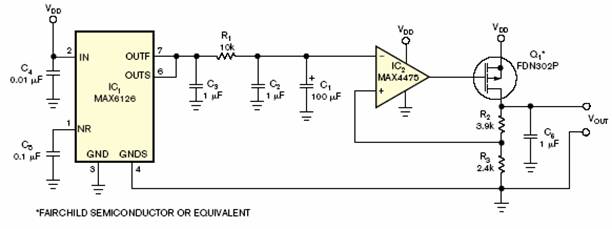
Figure 1 This low-dropout-voltage regulator features a noise floor of only 6 nV/Ö Hz, making it an ideal power source for low-noise oscillators.
Many low-dropout-voltage regulators see service in electronic systems, but relatively few are designed for low-noise operation. (For example, Maxim’s MAX8887 achieves a noise voltage of approximately 42 uVrms (10Hz-100kHz). However, certain applications, such as high quality MC preamplifiers, demand even lower levels of power-supply noise. To reach this level, the circuit in Figure 1 combines lownoise components and extra filtering to achieve an output noise floor of only 6nV/√Hz. Voltage reference IC1, a Maxim MAX6126, features low output noise (35nV/√Hz with C3=1uF). Lowpass filter R1-C1 further reduces this noise by attenuating noise frequencies above IC1’s 0.16-Hz cutoff frequency. The filtered reference voltage drives the inverting terminal of error amplifier IC2, a Maxim MAX4475, which regulates the output voltage by means of Q1, a P-channel power FET source follower. Feedback resistors R2 and R3 determine the output voltage as follows:
 .
.
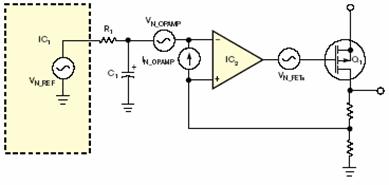
Figure 2 This simplified version of Figure 1 highlights noise sources for analysis.
The simplified noise-analysis diagram illustrates the components’ noise contributions (Figure 2). Lowpass filter R1-C1 attenuates high-frequency noise on the voltage reference’s output. The op amp’s noise current, 0.5 fA/ÖHz, is negligible with respect to its voltage noise, 4.5 nV/ÖHz. The referencenoise source adds to the op-amp voltage noise because they effectively connect in series. The MOSFET’s noise contribution appears at Q1’s input.
The noise at IC2’s inverting terminal equals the noise at its noninverting terminal:
 and
and

where VN_OUT represents the low-dropout circuit’s output noise, VN_REF represents the reference noise, VN_OPAMP represents the op amp’s inputreferred noise, and H(f) represents the R1-C1 lowpass filter’s transfer function. If a noise frequency of interest falls well below the filter’s cutoff frequency, the reference noise is negligible, and the lowdropout circuit’s output noise comprises only the op amp’s noise multiplied by the closed-loop gain. The feedback loop suppresses VN_FET, the MOSFET’s noise contribution, which therefore can’t contribute to the output noise. For frequencies within the loop’s bandwidth, the low-dropout circuit also rejects ripple and noise voltages that the power supply introduces.
Every high-end fun meet already this apparently very simple, but in the reality complicated problem: to make very low noise power supply for his/her preamplifier. In practice you can find two big class of regulators - switching and linear. The advantages of switching supplies revolve around low weight, low material cost, and their ability to actively regulate at no additional cost. Bur that is just apparently!

Figure 3 A noise-density-versus-frequency plot for the lowdropout circuit in Figure 1 is 38 dB lower than that of a conventional low-noise, low-dropout-voltage regulator—in this case, a Maxim MAX8887.
Figure 3 shows a plot of noise density versus frequency for the circuit of Figure 1, which exhibits a noise floor of about 6 nV/ÖHz at 1 kHz. For comparison, the plot shows the noise-measurement instrument’s noise floor and a typical low-dropout circuit’s much higher noise density—for example, 500nV/√Hz at 1 kHz for the MAX8887 low-noise, low-dropout circuit.
2. Low noise
regulator with 0-13V/1A output, 1uV noise (LC Audio Ltd.)
Figure 4 shows an other low noise voltage regulator made with common components, published by LC Audio Ltd. This DC Dual Tracking Regulator is perfect to supply RIAA/MC preamplifier with clean noise free power. A blue LED is used to pre regulate the voltage for the main reference, and gives an improvement in noise supression of 25 dB. Total noise rejection is 90 dB, and internal noise sources are in the magnitude of 1uV or 70-100 times better than a standard 7812/7912. The output can be regulated between 0-13V, max. 1A. Inserting an additional RC network after LM329, that noise can be more decreased.
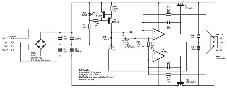
Figure 4 Low voltage regulator using comon components
3. Low noise regulator for 15V supply, 20-nV/√Hz noise floor
The following circuit (Figure 5 ) was designed by Wenzel Inc. is also for filtering 15 volt supplies. The shunt will greatly reduce white noise, spurious signals, and line-related signals on the power supply; the attenuation can exceed 40 dB with careful construction. The values are not critical except that the gain of the amplifier should be very near the ratio of the transistor emitter resistor to the series shunt resistor. In this case the gain is 15/0.05 = 300. Actually the gain is 301 with the indicated values so a 299k resistor would be theoretically better but the resistor tolerances and the actual resistance in the 0.05 ohm shunt path will cause more variation. One of the gain resistors may be made variable to allow the performance to be tweaked for the deepest null, if desired. Choose a low noise metal foil or wirewound potentiometer for best results. Standard fixed values will give excellent noise reduction sufficient for most applications. The LM833 is an excellent choice but many other low noise op-amps will work well. Is recommended to select an op-amp with a high bandwidth and low input noise voltage. A higher value shunt resistor may be used if the voltage drop can be tolerated.. The LM833 is a dual op-amp so two shunts may be implemented with the one package for filtering two different supplies or for cascading two shunts for additional line rejection and noise reduction. The noise shunt provides no load rejection beyond the rejection provided by the source regulator through the 0.05 ohm resistor.
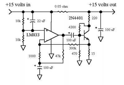
Figure 5 Low voltage regulator with shunt using comon components (by Wenzel Inc.)
The following graph shows the performance of the noise shunt when powered by a three-terminal regulator. The regulator's noise is 330 nV/ÖHz at 100 hertz and the circuit reduces this noise to 20 nV. This 24 dB reduction is achieved without any selected values and with no particular attention paid to the layout. The one potential problem area is the grounding; heavy ground traces or even ground plane are recommended. The ultimate rejection of the circuit is better than the apparent rejection in the plot; low frequency performance is impacted by the size of the coupling capacitors and the noise floor is limited by the performance of the LM833 and resistor noise.
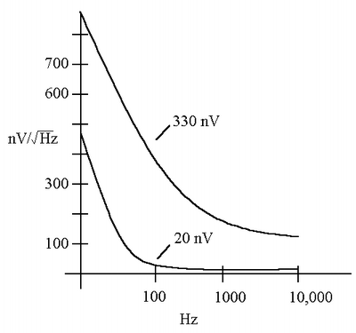
Figure 6 A noise-density-versus-frequency plot for the low dropout circuit in Figure 5 is 24 dB lower than that of a conventional 3 pin regulator (by Wenzel Inc.).
That ideea are useful in case of any low serial regulator, their noise are much higher than of this circuit made with reference voltage IC and low noise opamp.
4. Super Teddy Regulator
This regulator was designed by Teddy Prado, and in details are described on his webpage. The schematics can be seen below:
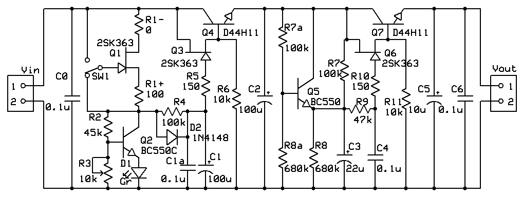
Figure 7 The Super Teddy Regulator - positive voltage part. SW1 are used just for negative pert!
Consists from two stages, a voltage regulator and a low pass filter.
The
regulator stage consists of a current source and a
bipolar
transistor configured as a voltage reference(acting like a
Zener). Q1
and R1
act as current source (for the positive version Lnk1 should be
positioned at
the "+" position. Use R1+ and a link instead of R1-). With a 2SK363BL
and 100R the current is around 1.5-2mA. Q2,
D1,
R2, and R3 act as voltage reference. Teddy's opinion: Zener
diodes are extremely noisy, even monolithic voltage references and
shunt
regulators such as the LM329.
The
voltage at the base of Q2 is about 2.42V (the LED voltage + the
transistor
Vbe), which means that about 0.57mA flows through R3 (when set to
4.2K). The
voltage on the Collector of Q2 is equal to the Vb + Ir3 x R2. Using 42K
for R2
we get 2.4 + 0.00057x42000 equals around 27V. In practice the voltage
varies
and a 10K trimmer is recommended for fine tuning. Comparing
to a Zener diode or
monolithic voltage references, a transistor based voltage reference has
high
output impedance, but since there is no current through the gate of Q3
the
output impedance has no effect in this circuit. On the other hand this
voltage
reference has a significantly lower noise level which is much more
important in
this context. The voltage reference is followed by a first order low
pass filter Gyrator that
cleans part of the ripple. R6 is a bias resistor, it should be set to
allow
1-3mA through Q3. The purpose of this resistor is to force Q3 into its
linear
region where it performs better. The diode is used to accelerate the
charging of C1.
The filter stage is a first order low pass filter consisting of R7, C3 and C4, and Q6 and Q7 acting as Gyrator. R7 and R8 make a voltage divider and should be calculated to allow a minimal dropout of 2V on the filter stage. The negative Vgs of Q6 is approximately equal to the positive Vbe of Q7, which means that the output voltage is approximately the same as the voltage of the voltage divider. R7a, R8a, and Q5 are optional and act as accelerator, that is, they charge C3 rapidly and disconnect as soon as C3 reaches the final voltage defined by R7 and R8. The accelerator circuit is required when powering DACs, clocks, and other CD circuits where start time is critical.
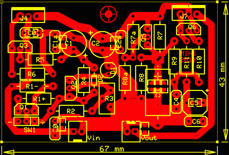
Figure 8 The Super Teddy Regulator PCB
A 2SK363BL has a current limit of about 12mA, and the D44H11 has a hfe of about 200, the combination of the two allows a maximum current of around 2.5A. The D44H11 can withstand up to 10A and 50W so in practice the circuit is protected against short circuits at the output. Note: using jfets with higher Idss will allow higher currents!
C3 is the most critical capacitor, need low leakage capacitors, ex. dry tantalum capacitors. Personally I decide to use a Vishay MKT 22uF. Ceramic capacitor should be COG/NPO type.The
calculation of R3 is quite
complex, I recommend using a 10K trimmer to set the exact value.
Assuming a 10K trimmer, R2 should be calculated as follows:
- For output voltage between 20-30V use around 50K
- For output voltage between 10-20V use around 25K
- For output voltage below 10V use around 10K
R8 and R8A should be calculated to allow at least 2V dropout.The
dropout on the second stage
(Vdo) can be calculated using the following formula:
Vdo =
Vout / ((R7+R8)/R7) -1)
Using
100K for R7: Vdo = 100 * Vout / R8 or R8 = 100 * Vout / Vdo
For a dropout of 2.5V R8 = 40 * Vout , where R8 is in kOhm.
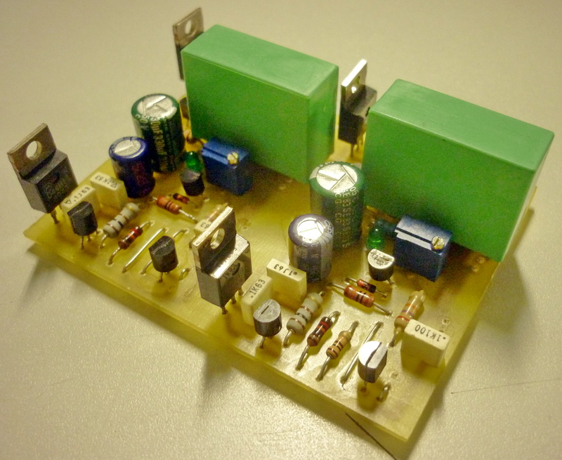
Figure 9 Built regulator (for positive and negative supply) - component side.
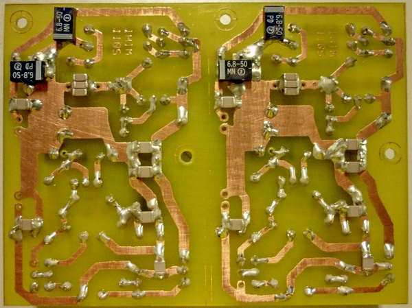
Figure 10 Built regulator (for positive and negative supply) - solder-side.
The output
capacitor are formed from 2 pcs of 6.8uF/50V Ta. All used MLCC capacitors are
22nF/50V NPO type.
Negative version of Regulators:
The
SuperTeddyReg PCB was designed
to allow implementation of either positive or negative version on the
same PCB - by one jumper as SW1 and replacing/eliminating some
components:
- Use a wire link instead of R1+
- Use a wire link in the oposite position of SW1 (like using a switch)
- Reverse the polarity of all electrolytic and Tantalum capacitors
- Reverse the LED polarity
- Reverse Q1
- Use P channel jfet for Q3 and Q6 (e.g. Toshiba J74).
- Use BC560C for Q2
- Use D45H11 for Q4 and Q7
- Use BC560 for Q5