Function generator with MAX038
Sometimes, to test operational amplifiers' performance, to be used in audio, it would have been nice to test them at over 10MHz. For that reason, I wanted to design a simple and low-cost one, a high-speed function generator with a sinus waveform and a square and triangular one.
For the design idea, I started looking on the web and chose the MAX038 chip from Maxim. A complete 20MHz sine/square/triangle function generator in a single chip! While it is possible to build a complete function generator using just the MAX038, I found that it needed just a little bit more circuitry to make it into a fully-fledged function generator design.
The final design described here is capable of producing sine, square, triangle, and TTL level waveforms at up to and beyond 20MHz. Normally, an analog function generator capable of this frequency would be very expensive and very complex. But as you can see, this entire design consists of little more than 4 ICs for the generator and 2 for the power supply.
Please note, this project has been designed for the highest possible frequency coverage, and for the lowest possible distortion level, with that, it should be fine for any kind of application.

Figure 1 Bloc diagram and basic operating circuit of MAX038
Surprisingly, the MAX038 does not use any fancy techniques to produce frequencies from 1 Hz up to 20MHz or more. Instead, it uses a simple relaxation-type oscillator that operates by charging and discharging a capacitor (on pin 5) using a constant current. It is basically a dual slope integrator that produces a triangle wave the frequency of which is determined by the external oscillator capacitor and the input current at the Iin pin. This internal triangle wave is fed into an internal comparator to produce the square wave function. The sine wave function is produced by feeding the triangle wave into a sine wave shaping circuit that automatically corrects for the desired frequency, and produces a reasonably low distortion sine wave at a constant amplitude. The sine, square, and triangle waves are then fed into a multiplexer that selects which function to output through a low-impedance output buffer.
The MAX038 does all of the work in generating the actual waveform, so the rest of the circuits just tell which frequency to operate, and which type of waveform (sine/square/triangle) to produce.

Figure 2 The schematic of function generator
The output frequency is determined by three factors. The first one is the value of the oscillator capacitor on pin 5, which sets the frequency range that the chip will operate within. The second and third factors are the Current Input "Iin" (pin 10) and the Frequency Adjust "FAdj" (pin 8) pins. Somewhat contrary to its name, the Frequency Adjust pin is not the best way to adjust the output frequency. The output frequency is actually directly proportional to the current going into the Iin pin. The FAdj input is merely used for finer frequency adjustment (or for frequency modulation), as it only has about 70% of the adjustment range of Iin. The FAdj circuit adds a small temperature coefficient to the output frequency. For critical open-loop applications, I turned it off by connecting FAdj to GND (not Ref) through a 12kohm resistor (R8 in Figure 2).
The current into Iin used to adjust the output frequency can range from approximately 2uA to 750uA, but for optimal performance must be between 10uA to 400uA - recommended by the datasheet. The Iin pin acts as a virtual ground, and thus it is a simple matter of applying a positive voltage via a resistor to Iin. This produces a current into Iin which can be simply worked out using Ohm's law. In fact, the output frequency can be related by the simple formula: Fo (MHz)= Iin(uA)/Cf(pF) Where Cf is the value of the oscillator capacitor on pin 5. This formula assumes that FAdj is at zero volts. Used capacitors for 6 frequency ranges: 22pF, 220pF, 2.2nF, 22nF, 220nF and 2.2uF. Excepting 22pF (NPO ceramics) and 220pF (polystyrol), the rest of capacitors are polypropylene type.
The voltage on DAdj (pin 7) controls the waveform duty cycle (defined as the percentage of time that the output waveform is positive). If VDAdj = 0V (selected by SW2), the duty cycle is 50%. Varying this voltage from +2.3V to -2.3V via P1 causes the output duty cycle to vary from 15% to 85%, about -15% per volt. Voltages beyond ±2.3V can shift the output frequency and/or cause instability.
SYNC (pin 14) is a TTL/CMOS-compatible output that can be used to synchronize external circuits. The SYNC output is a square wave whose rising edge coincides with the output rising sine or triangle wave as it crosses through 0V. When the square wave is selected, the rising edge of SYNC occurs in the middle of the positive half of the output square wave, effectively 90 degrees ahead of the output. The SYNC duty cycle is fixed at 50% and is independent of the DAdj control. Because SYNC is a very high-speed TTL output, the high-speed transient currents in DGND (pin 15) and DV+ (pin 16) can radiate energy into the output circuit, causing a narrow spike in the output waveform. (This spike is difficult to see with oscilloscopes having less than 100MHz bandwidth). The inductance and capacitance of IC sockets tend to amplify this effect, so sockets are not recommended when SYNC is on. SYNC is powered from separate ground and supply pins (DGND and DV+), and it can be turned off by making DV+ open circuit with SW3. If synchronization of external circuits is not used, turning off SYNC by DV+ opening eliminates the spike.
The MAX038 contains a TTL/CMOS phase detector that can be used in a phase-locked loop (PLL) to synchronize its output to an external signal - which is not used in my design. Because that internal phase detector is not used, PDI and PDO are connected to GND.
To eliminate any distortions regarding the load, I use an opamp as output buffer - AD847, a video buffer circuit.
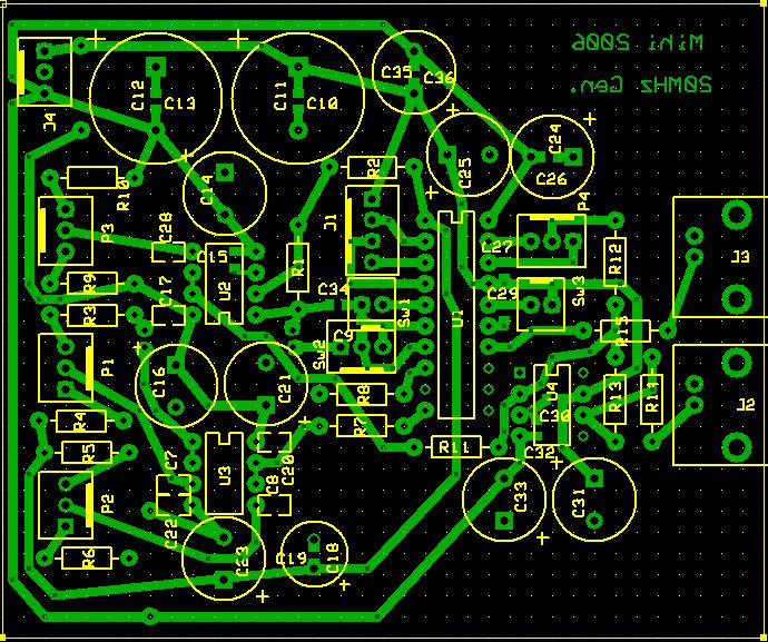
Figure 3 Solder side of pcb
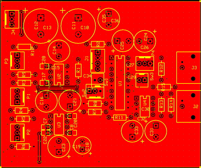
Figure 4 Cooper or component side of pcb
Realizing the full performance of the MAX038 requires careful attention to power-supply bypassing and board layout. I use a low-impedance ground plane, and all five GND pins are directly connected to it. V+ and V- are directly bypassed to the ground plane with 22nF NPO/C0G-type ceramic capacitors in parallel with 47uF ultra-low impedance electrolytic capacitors. To keep capacitor leads short (especially with the 22nF ceramics) to minimize series inductance, they are connected to MAX038's pins directly on the ground-plane. Because SYNC can be used (switched on/off via SW3), DV+ is connected to V+, DGND must be connected to the ground plane, and one 22nF and a 1uF tantalum capacitor are connected between DV+ and DGND (pins 16 and 15). It is not necessary to use a separate supply or run separate traces to DV+.
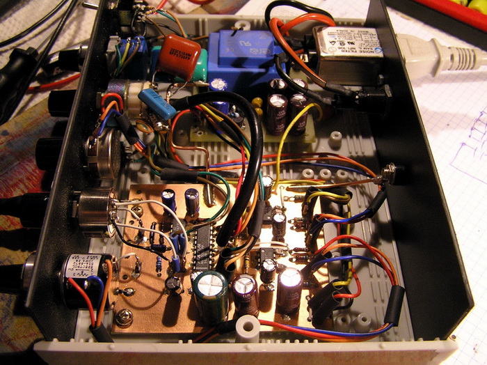
Figure 5 A look inside
The power supply circuit comprising 78L05 and 79L05 is a standard +/- 5V regulated supply fed by a full wave rectified AC input.
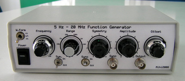
Figure 6 The final function generator
Conclusion: the MAX038 integrated circuit is the most performant one-circuit function generator, which manufacturing was unfortunately stopped - for that reason the acquisition is difficult. Sincerely I cannot understand the reason why was stopped, or why other manufacturers did not develop a similar integrated circuit.