Headphone
amplifier with TPA6120A2
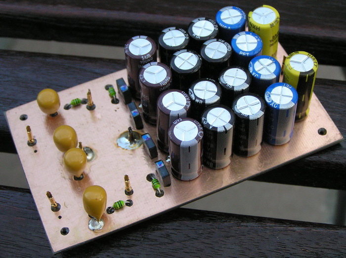
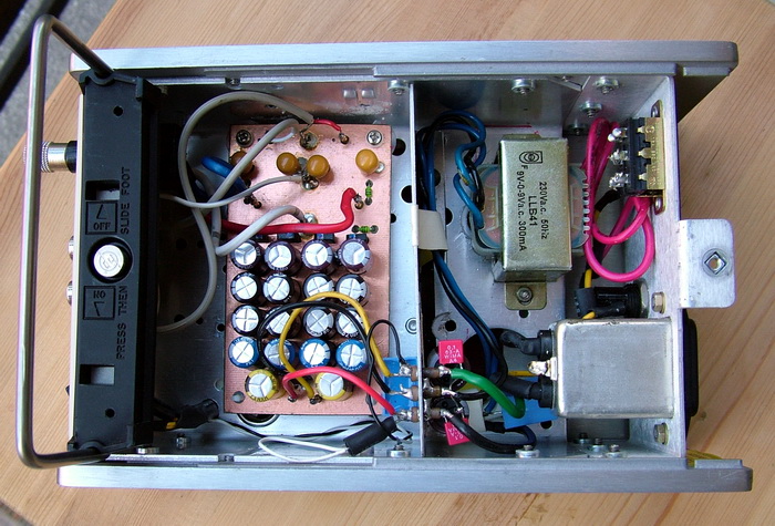
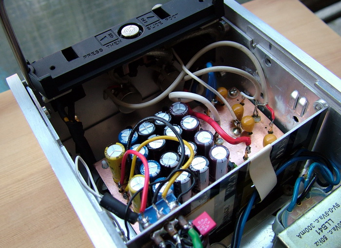
About schematic: the output is protected with R19, R20 (10 ohms), because the minimum load impedance must be 8 ohms, and can serve to protect the amplifier from any capacitance on the output path. The amplifier is powered from 2x11.5V using just passive filtering to increase the power's dynamic response (I use 48 capacitors, in total more than 30mF - for the whole headamp). The current feedback's advantage is the low voltage noise, high open-loop gain throughout a large frequency range, and low distorsion, but for this reason, the PCB can be designed carefully. Apparently seems to have 2 independent operational amplifiers into a single chip with separate powering, but they are not completely independent! Can be followed the next rules recommended by manufacturer:
- when both amplifiers are used, the power supplies must be same - in other cases the device not operate properly (for this reason on the recommended evaluation-board under IC they are directly connected,
- when just one amplifier is used, it must be the left one.
the power supply decoupling is very essential, that means the C11,12,13,14 capacitors must be placed as close as possible to power pins of IC, and can be low ESR type (I use 4 pcs of 0.47uF/16V 0603 size B type TDK MLCCs).
Other design recommendations:
- the value of the feedback resistor must be chosen from the specification's diagrams. I select 1kohm, to have noise optimum level and enough bandwidth, but must be a very good quality type (ex. Dale/Vishay)!
- regarding high slew-rate and current feedback operation, must be avoided any kind of capacitor in feedback, and output circuit, because can make oscillations! Also, the PCB should be designed in that way to avoid unwanted capacitors in the above-mentioned circuits.
- the source always can be connected to the input and must have low impedance, in other cases immediately starts the oscillation. To avoid that, I use an opamp as an input buffer, AD8065 IC from Analog Devices.
- an input series resistor is recommended to prevent the noninverting-input from source capacitance. 50 ohms was recommended, but I have just 110 ohm at "home's stock", and I use two connected in parallel.
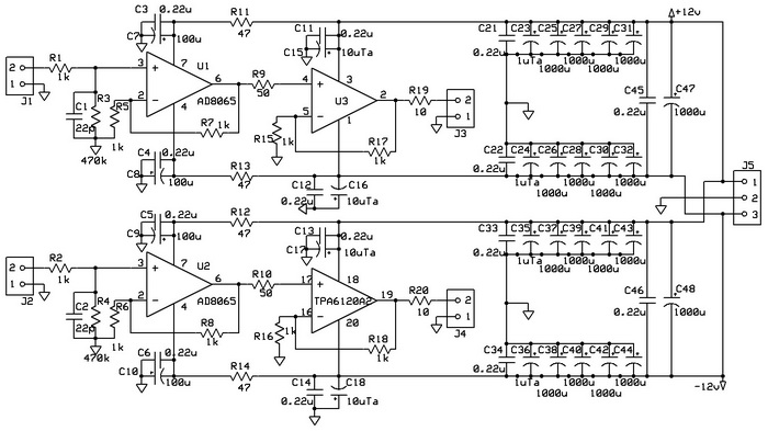
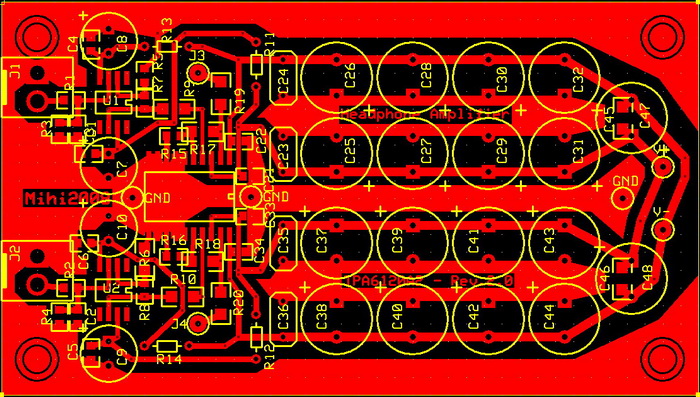
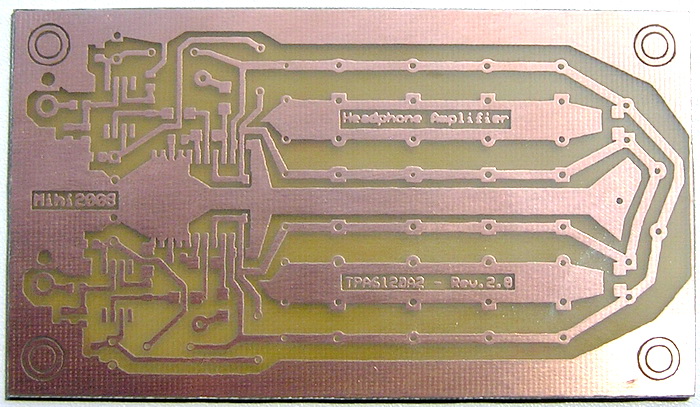
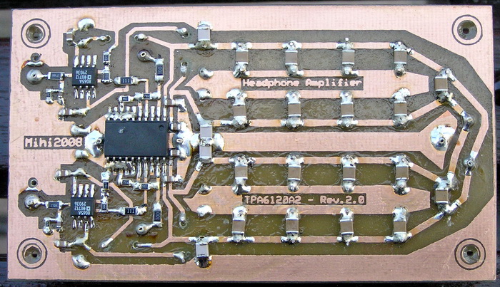
The amplification (2x) are set by R15, R17 and R16, R18. Both amplifiers powering are made with separate buffers (2x4 pcs of low ESR 1000uF/25V Sam Yong type NXH series capacitors for each amplifier - total 16 pcs) to increase channel separation and dynamics. The proper layout is crucial, but the specification gives a good guideline. Is mentioned all 3 resistors (input, feedback, and output) terminals should be as close as possible (the layout paths must be the shortest) to IC's pins. The PCB was designed with ExpressPCB - a freeware program. Here is the result:
Measured parameters:
Output DC offset: < 1mV
Noise (Max volume, no input) (Vrms): 6uV
S/N (Max volume, 1kHz): 112dB
Channel separation (Max Volume on 32ohms): 119dB
Gain Voltage: x2.0
Zin (without/with volume control potentiometer): 469kΩ/10kΩ
Output power: >900mW on 32 ohm, >80mW on 600 ohm
THD at 20kHz: lower than 0.002% measured at Pmax on 32 ohm
IC's temperature at full power after 4 hour operation: 36 º C
Power supply ripple noise (max Pout at 32 ohm): < 0.1mV RMS